The Challenges of Micro LED Display Technology

What is Micro LED?
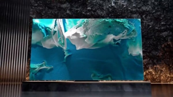
Micro-LED display technology is a self-luminous display technology, through the array of micro-level LED light-emitting devices (μLED) integrated into the active addressable driver substrate, in order to achieve individual control and lighting, so as to output the display image. The micro-LED display has many advantages such as self-illumination, high resolution, low response time, high integration, high reliability, etc., and small size, high flexibility, easy to disassemble and merge, can be used in any existing display applications from small to large size. In many application scenarios, compared with liquid crystal displays (LCD) and organic light-emitting diode displays (OLED), Micro LED displays can play a more excellent display effect.
Micro LED epitaxial technology challenges
Substrate Material Selection
Wavelength uniformity control
Micro-LED display technology is a self-emitting display technology. In high-resolution display applications, the difference in color rendering caused by the uneven emission wavelength of Micro-LEDs can greatly affect the display effect. To ensure the display effect, the standard deviation of wavelength variation of Micro-LED epitaxial wafers needs to be controlled at 0.8 nm or less. Therefore, the control of airflow and temperature uniformity is particularly important in the epitaxial growth of InGaN/GaN quantum wells by metal-organic chemical vapor deposition (MOCVD).
Optimizing the airflow uniformity in the MOCVD epitaxial growth process plays a crucial role in the improvement of LED wavelength uniformity. At present, Prismo UniMax, the latest domestic micro MOCVD equipment, adopts zonal temperature control technology to ensure the temperature field balance throughout the epitaxial growth and uses a series of strain control technologies such as MO source and airflow uniformity to enhance the wavelength uniformity of LED epitaxial wafers to meet the demand of micro-LED display. For micro-LED applications with high requirements for wavelength uniformity, the graphite tray design can be optimized to make it have a certain curvature to better match the epitaxial wafer warpage during the epitaxial growth process to achieve further improvement of temperature uniformity control.
Defect control
Dislocations as non-radiative composite centers and leakage channels can significantly affect the chip Micro-LED performance. Due to the small size of Micro-LED and low injection current density, its optoelectronic performance is very sensitive to the dislocation density. Currently, patterned substrate technology and buffer layer technology are more often applied to the heterogeneous epitaxial growth of GaN on sapphire or silicon substrates to reduce the dislocation density and improve the crystal quality. The homogeneous epitaxy technology on high-quality GaN substrate can effectively reduce the dislocation density of LED epitaxial wafers.
