SMD and COB LED Technology Difference
When it comes to LED display packaging technology, we most often hear about SMD technology and COB technology, so what are these two technologies, and what are the differences? This article takes you to a glance at the end.
Process Introduction
SMD technology route is the light-emitting chip (wafer) packaged into lamp beads, the lamp beads are welded to the PCB board to form a unit module and finally spliced into a whole LED screen.
COB technology route is to send the light chip (wafer) directly welded to the PCB board, and then the overall lamination to form a unit module, and finally stitched into a block of LED screen.
Product differences
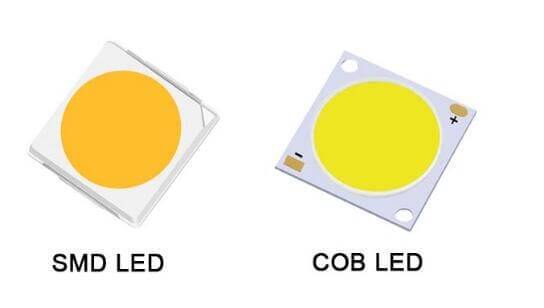
Image differences
SMD screen lamp beads for a single light, showing the effect of point light source, COB screen due to the overall lamination above the light-emitting chip, the light source after the lamination scattering, and refraction into a surface light source. Surface light source compared to point light source overall visual perception is better, no particle sense when watching, and can reduce the light source on the human eye stimulation, more suitable for a long time close viewing.
COB screen using a new process after the overall package, the contrast ratio can be higher, up to 20000:1 or more, SMD screen contrast ratio will not exceed 10000:1, compared to the frontal viewing COB screen viewing effect is closer to the LCD screen, the color is bright and vivid, better detail performance.
However, because the COB screen can not be similar to the optical performance of the single lamp beads as SMD screen sorting, the factory needs to do the whole screen correction, although the frontal viewing effect is excellent, the large angle side view is prone to color inconsistency.
Reliability difference
SMD technology LED screen, because the light-emitting chip is first encapsulated and then mounted, the overall protection is weak, easy to knock the light off the light, waterproof, moisture-proof, dustproof performance is poor, can not be wiped, but the site maintenance is convenient, conducive to later maintenance.
COB technology LED screen, the use of chips directly after the overall lamination, the overall protection is better, the frontal protection level up to IP65, can effectively waterproof, moisture-proof, and anti-knock, you can use a wet towel for cleaning, but due to the overall lamination, the site can not be repaired, need to return to the factory to use professional equipment maintenance, more inconvenient.
Energy efficiency differences
SMD screen mainstream products within the light-emitting wafer beads are mostly a positive installation process, the light source above the lead shield, while COB screens are mostly a flip-flop process, the light source is not shielded, so to achieve the same brightness, COB screen power consumption is lower, with better use of economic type.
In addition, due to the low permeability of epoxy resin used in SMD lamp bead packaging, the COB screen adopts a higher permeability of the overall lamination, which further enhances the economic use of the COB screen.
Cost difference
SMD production process and procedures are relatively complex, but due to the low technical threshold, there are more than a thousand manufacturers in the country, the competition is more adequate, and the technology development is more mature.
COB production process technology threshold is high, there are only less than twenty manufacturers in the country that have the ability to develop production and manufacturing.
COB technology is still in rapid development, and although its theoretical cost is lower than SMD screen, due to the low product yield, the current cost of COB screen compared to SMD screen in more than 1.2 pitch still has a certain disadvantage.